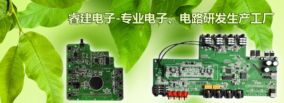
Welcome to the official website of Dongguan Ruijian Electronic Technology Co., Ltd.!


[PCB Information Network] The cause of the tin tip phenomenon of the lead components during the wave soldering time: During the soldering process, as the solder wets and covers the surface of the circuit board, most of the flux on the circuit board will be washed away, leaving behind the help The flux is located between the PCB board and the tin wave. When the PCB board leaves the tin wave, the flux remaining on the PCB board will prevent the oxidation of the solder. If the space between the solder joints is relatively small, there will not be too much flux remaining in this process, so it is almost impossible to prevent the solder from oxidation. As a result, when the tin wave separates from the PCB board, the solder will oxidize and form an oxide layer on the surface. In the final stage of separation, the surface tension of the liquid solder will leave part of the solder on the pins of the component; if this part of the solder surface is oxidized, the solder will be wrapped in the oxide layer to form a tin tip. This phenomenon will be more obvious if there is a larger area covered by solder and almost no flux can help prevent oxidation. Therefore, we can understand why long pins are more likely to cause tin spikes, because only the flux remaining on the surface of the PCB can help prevent oxidation. In the process of separating the PCB from the tin wave, the long pins are separated from the PCB. The surface of the board is far away, and the anti-oxidation effect of the flux on the surface of the PCB board on the pins is obviously weakened. In the same way, the tin tip phenomenon is also prone to occur in the place where the pad area is large on the PCB board. Due to the heat dissipation effect, the solder joints on the shielding cover are also prone to tin tip phenomenon. If the heat brought by the solder to the solder joint is quickly absorbed by the shield, the solder will solidify almost immediately after it is separated from the tin wave. As a result, the solidified tin cannot flow back to the solder joint to form a tin tip. The solution to the tin tip phenomenon of long-term pin components during wave soldering: Make the protruding component pins shorter, so that the flux remaining on the PCB can still protect it from oxidation. Generally speaking, increasing the amount of flux will not work, because when the PCB board is over the tin wave, these fluxes are likely to be washed away; of course, more flux helps to wet the pads ; If you use a flux with a strong adsorption force to the PCB board, it may help prevent the tin tip phenomenon from occurring. When the PCB board passes through the tin wave, adding inert gas to cover or creating an environment that helps reduce oxidation can also avoid the phenomenon of tin spikes. If the tin tip is caused by the heat dissipation effect near the solder joint, the solder joint design must be optimized.